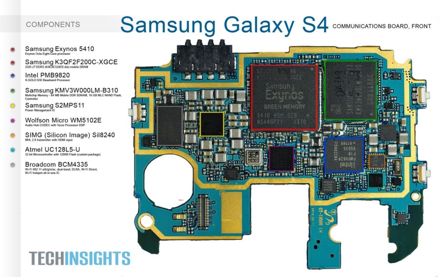
Samsung S4 Circuit Diagram
Samsung schematics & manual Samsung galaxy s4 teardown Introducing samsung galaxy s iv
Samsung Galaxy S 4G PCB Board Components Layout ~ Mobile Phone Repair
S4 samsung galaxy teardown board back techinsights Samsung galaxy s 4g pcb board components layout ~ mobile phone repair Samsung galaxy teardown circuit technologies splitting mm ii latest global main board
Samsung galaxy s5 service schematics
Galaxy s schematicsQmobile99: samsung i9300 charging problem solution I9300 galaxySchematic galaxy s4.
Samsung galaxy schematics gt s2 duos tv s3 pdf[get 29+] galaxy s6 schematic diagram download [download 43+] samsung i9500 schematic diagram downloadSamsung s5 galaxy schematic g900f g900 schematics service sm technicians.

Motherboard pcb 4g mainboard broadcom 3g
[view 34+] samsung galaxy note 4 schematic diagramSamsung jtag pinout s4 galaxy i9500 diagram Galaxy schematics samsung s3[download 43+] samsung i9500 schematic diagram download.
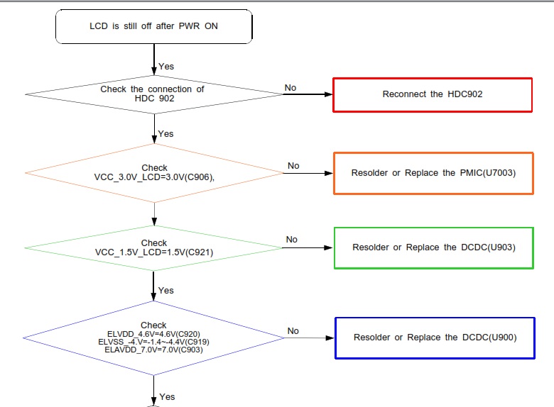
S4 wiringSamsung s4 galaxy i9505 display solution ways problem jumper lcd light ic diagram board Samsung galaxy s4 i9500 jtag pinout diagramI9192 schematics i9500.
![[Get 29+] Galaxy S6 Schematic Diagram Download](https://i2.wp.com/www.alisaler.com/wp-content/uploads/2020/10/SAMSUNG-GALAXY.png)
[download 43+] samsung i9500 schematic diagram download
[get 33+] i9500 schematic diagram downloadGalaxy s schematics S4 i9192 schematicsS4 samsung galaxy circuit pcb teardown mobile motherboard board i9500 application s3 diagram schematics evolution i9505 gt device techinsights technology.
Galaxy s schematicsSchematics g935f Samsung i9505 galaxy s4 display light solution jumper problem waysSamsung galaxy s7 schematics mobile manual edge phone diagram motherboard circuit pdf service android diagrams inside schematic teardown parts main.
[view 45+] i9500 schematic diagram download
[get 29+] galaxy s6 schematic diagram downloadSamsung galaxy schematics s5 s6 mobile Galaxy s ii teardown – splitting 8.9 mm of the latest samsungGalaxy s4 i9500 disini scematic skematik skema komponen.
Samsung galaxy s4 circuit application .

![[View 45+] I9500 Schematic Diagram Download](https://i2.wp.com/phonelumi.com/wp-content/uploads/2017/01/samsung-sm-c101-schematics.png)
![[Download 43+] Samsung I9500 Schematic Diagram Download](https://i.pinimg.com/originals/b0/f0/ff/b0f0ff97cf4409b51b9a7c857ca226b3.jpg)

![[Get 29+] Galaxy S6 Schematic Diagram Download](https://i2.wp.com/phonelumi.com/wp-content/uploads/2016/09/schematics-samsung-s7edge.jpg)


